- 您现在的位置:买卖IC网 > Sheet目录3896 > PIC16F505T-I/SL (Microchip Technology)IC MCU FLASH 1KX12 14SOIC
2009 Microchip Technology Inc.
DS41236E-page 13
PIC12F508/509/16F505
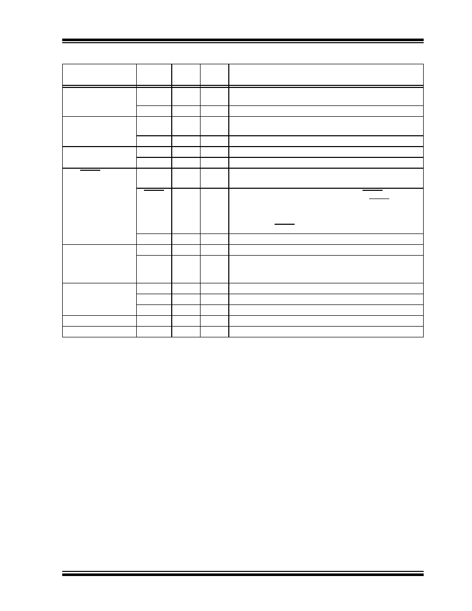
TABLE 3-2:
PIC12F508/509 PINOUT DESCRIPTION
Name
Function
Input
Type
Output
Type
Description
GP0/ICSPDAT
GP0
TTL
CMOS Bidirectional I/O pin. Can be software programmed for internal
weak pull-up and wake-up from Sleep on pin change.
ICSPDAT
ST
CMOS In-Circuit Serial Programming data pin.
GP1/ICSPCLK
GP1
TTL
CMOS Bidirectional I/O pin. Can be software programmed for internal
weak pull-up and wake-up from Sleep on pin change.
ICSPCLK
ST
CMOS In-Circuit Serial Programming clock pin.
GP2/T0CKI
GP2
TTL
CMOS Bidirectional I/O pin.
T0CKI
ST
—
Clock input to TMR0.
GP3/MCLR/VPP
GP3
TTL
—
Input pin. Can be software programmed for internal weak
pull-up and wake-up from Sleep on pin change.
MCLR
ST
—
Master Clear (Reset). When configured as MCLR, this pin is
an active-low Reset to the device. Voltage on MCLR/VPP must
not exceed VDD during normal device operation or the device
will enter Programming mode. Weak pull-up always on if
configured as MCLR.
VPP
HV
—
Programming voltage input.
GP4/OSC2
GP4
TTL
CMOS Bidirectional I/O pin.
OSC2
—
XTAL
Oscillator crystal output. Connections to crystal or resonator in
Crystal Oscillator mode (XT and LP modes only, GPIO in other
modes).
GP5/OSC1/CLKIN
GP5
TTL
CMOS Bidirectional I/O pin.
OSC1
XTAL
—
Oscillator crystal input.
CLKIN
ST
—
External clock source input.
VDD
—
P
Positive supply for logic and I/O pins.
VSS
—
P
Ground reference for logic and I/O pins.
Legend: I = Input, O = Output, I/O = Input/Output, P = Power, — = Not used, TTL = TTL input,
ST = Schmitt Trigger input, HV = High Voltage
发布紧急采购,3分钟左右您将得到回复。
相关PDF资料
PIC12F509T-I/SN
IC MCU FLASH 1KX12 8SOIC
PIC10F200T-E/OT
IC PIC MCU FLASH 256X12 SOT23-6
006200516230000
CONN FFC/FPC 16POS 1MM R/A SMD
006200516230000+
CONN FFC/FPC 16POS 1MM R/A SMD
40FMN-BMT-A-TF
CONN FMN HSNG 40POS SNGL NOR SMD
0781191309
CONN FFC/FPC 30POS .5MM VERT SMD
046214012010800+
CONN FPC VERTICAL 0.5 MM 12POS
006200514230000+
CONN FFC/FPC 14POS 1MM R/A SMD
相关代理商/技术参数
PIC16F505T-I/SL040
制造商:Microchip Technology Inc 功能描述:MCCPIC16F505T-I/SL040 14 PIN 1.5 KB F
PIC16F505T-I/ST
功能描述:8位微控制器 -MCU 2 KB 72 RAM 12 I/O RoHS:否 制造商:Silicon Labs 核心:8051 处理器系列:C8051F39x 数据总线宽度:8 bit 最大时钟频率:50 MHz 程序存储器大小:16 KB 数据 RAM 大小:1 KB 片上 ADC:Yes 工作电源电压:1.8 V to 3.6 V 工作温度范围:- 40 C to + 105 C 封装 / 箱体:QFN-20 安装风格:SMD/SMT
PIC16F506-E/MG
功能描述:8位微控制器 -MCU 1.5KB 67 RAM 12 I/O RoHS:否 制造商:Silicon Labs 核心:8051 处理器系列:C8051F39x 数据总线宽度:8 bit 最大时钟频率:50 MHz 程序存储器大小:16 KB 数据 RAM 大小:1 KB 片上 ADC:Yes 工作电源电压:1.8 V to 3.6 V 工作温度范围:- 40 C to + 105 C 封装 / 箱体:QFN-20 安装风格:SMD/SMT
PIC16F506-E/P
功能描述:8位微控制器 -MCU 1.5KB FL 67 RAM 12I/O Comp Ext Temp RoHS:否 制造商:Silicon Labs 核心:8051 处理器系列:C8051F39x 数据总线宽度:8 bit 最大时钟频率:50 MHz 程序存储器大小:16 KB 数据 RAM 大小:1 KB 片上 ADC:Yes 工作电源电压:1.8 V to 3.6 V 工作温度范围:- 40 C to + 105 C 封装 / 箱体:QFN-20 安装风格:SMD/SMT
PIC16F506-E/SL
功能描述:8位微控制器 -MCU 1.5KB Flsh 67RM 12IO Comp 8B ADC Ext Temp RoHS:否 制造商:Silicon Labs 核心:8051 处理器系列:C8051F39x 数据总线宽度:8 bit 最大时钟频率:50 MHz 程序存储器大小:16 KB 数据 RAM 大小:1 KB 片上 ADC:Yes 工作电源电压:1.8 V to 3.6 V 工作温度范围:- 40 C to + 105 C 封装 / 箱体:QFN-20 安装风格:SMD/SMT
PIC16F506-E/ST
功能描述:8位微控制器 -MCU 1.5 KB Flash 67RAM12 I/O 8bit ADC RoHS:否 制造商:Silicon Labs 核心:8051 处理器系列:C8051F39x 数据总线宽度:8 bit 最大时钟频率:50 MHz 程序存储器大小:16 KB 数据 RAM 大小:1 KB 片上 ADC:Yes 工作电源电压:1.8 V to 3.6 V 工作温度范围:- 40 C to + 105 C 封装 / 箱体:QFN-20 安装风格:SMD/SMT
PIC16F506-I/MG
功能描述:8位微控制器 -MCU 1.5 KB Flash 73 RAM 12 I/O RoHS:否 制造商:Silicon Labs 核心:8051 处理器系列:C8051F39x 数据总线宽度:8 bit 最大时钟频率:50 MHz 程序存储器大小:16 KB 数据 RAM 大小:1 KB 片上 ADC:Yes 工作电源电压:1.8 V to 3.6 V 工作温度范围:- 40 C to + 105 C 封装 / 箱体:QFN-20 安装风格:SMD/SMT
PIC16F506-I/P
功能描述:8位微控制器 -MCU 1.5KB 72 RAM 12 I/O Ind Temp PDIP14 RoHS:否 制造商:Silicon Labs 核心:8051 处理器系列:C8051F39x 数据总线宽度:8 bit 最大时钟频率:50 MHz 程序存储器大小:16 KB 数据 RAM 大小:1 KB 片上 ADC:Yes 工作电源电压:1.8 V to 3.6 V 工作温度范围:- 40 C to + 105 C 封装 / 箱体:QFN-20 安装风格:SMD/SMT